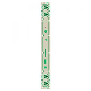
Tin Base Station Double Sided PCB ISO9001 UL Approved For Digital Products
2L Tin Base Station Antenna Double Sided PCB ISO9001 UL Approved
high frequency plate + super long size
Products are widely used in high-tech fields such as communications, power supplies, computer networks, digital products, industrial control, science and education, medical devices, and aerospace. HSX owns high-educated and experienced team and advanced production equipment.
The panel size of HSX factory's capability is max 740x500mm, but when the panel size is larger than 600mm, it will need to be review at first. And the minimum panel size that we can reach is 5*5mm.
The PCB thickness we can reach is from 0.2mm to 4.0mm, when the board thickness is lower than 0.2mm, or higher than 4mm, the board will need to be evaluated at first. (PS. When board thickness is equal to or less than 0.6mm, it will not apply for HASL surface finished)
The inner and outer layer's base copper thickness is smallest 0.3/0.5oz, and max 3oz.
FAQ:
Q1:Are you a factory or trade company?
A: Yes, we are the factory, we have independent quick turn prototype PCB manufacturing & big volume PCB production lines.
Q2:How about your PCB factory production capacity?
A: Our monthly production capacity is 50,000 square meter/month and 5000types/month.
Q3:If we have no PCB file/Gerber file, only have the PCB sample,can you produce it for me?
A: Yes,we could help you to clone the PCB. Just send the sample PCB to us, we could clone the PCB design and work out it.
Q4:How will you usually ship the PCB?
A: Usually for small packages, we will ship the boards by DHL,UPS,FedEx door to door service, we could use your shipping account to do collection or use our account to ship in DDU (import duty unpaid) delivery term.
For heavy goods more than 300kg, we may ship your PCB boards by ship or by air to save freight cost. Of course, if you have your own forwarder, we may contact them for dealing with your shipment.
Q5:What is your standard lead time for production?
A: Sample/prototype(less than 3sqm):
1-2 Layers: 3 to 5working days (fastest 24hours for quick turn services)
4-8 Layers: 7~12 working days (fastest 48hours for quick turn services)
Mass production (less than 200sqm):
1-2 Layers:7 to 12 working days
4-8 Layers:10 to 15 working days