HASL Hard Gold 2L Double Sided Flex PCB Board 4mil ENIG Finished
Flex PCB Board 2L Flexible Circuit Board Double Sided Circuit Flex Printed Circuit Board Assembly
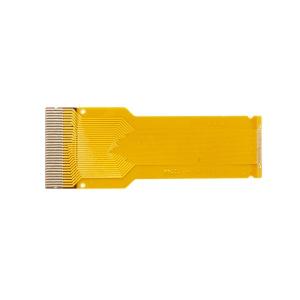
2L Flexible Printed Circuit Board
Flexible printed circuits are circuit boards that have the ability to bend or twist. From this assertion, it is obvious that they are distinguished by a flexible construction. That is why electronic engineers and designers use them in applications that demand for their qualities. They are also referred to as flex circuits and are mostly used in small electronic applications. Since they are characterized by their ability to bend, flexible printed circuits are made of flexible substrate such as polyimide. Another important quality of flexible printed circuits is that they have superior heat dissipation than printed circuit boards. It is this quality that makes it possible for the electronics that use it to stay in quality condition for a long time.
HSX products cover 1~32L FR-4 PCB, IMS PCB,HDI Boards, high frequency PTFE boards and Rigid-flex boards etc. It provides flexible quick turn production services (12 hours to72 hours), as well as small volume to big volume PCB manufacturing.Products are widely used in high-tech fields such as communications, power supplies, computer networks, digital products, industrial control, science and education, medical devices, and aerospace.
| FPC Technology Capability |
Attribute (All dimensions are mils unless
otherwise specified) | Mass Production (Yield≥
80%,Cpk≥1.33) | Small Amount(Yield≥60%, Key
Specification Yield≥80% | Sample |
| FPC(yes/no) | yes | yes | yes |
| Layer count/Structure, Max. | 2 | 4 | 6 |
| Size(L×W), Max. | 550mm*250mm | 550mm*250mm | 700mm*250mm |
| Nominal thickness (mm) | 0.1~0.5 | 0.1~0.5 | 0.1~0.8 |
| Thickness tolerance | ±10%(>0.3mm)/±0.03mm(≤0.3mm) | ±10%(>0.3mm)/±0.03mm(≤0.3mm) | ±10%(>0.3mm)/±0.03mm(≤0.3mm) |
| Surface finish type | ENIGENEPIGOPSI-SilverI-Tin HASLHard Gold | ENIGENEPIGOPSI-SilverI-Tin HASLHard Gold | ENIGENEPIGOPSI-SilverI-Tin HASL Hard Gold |
| Soft ENIG(yes/no) | no | no | no |
| Base material type | PI | PI | PILCPTK |
| Coverlay thickness (um) | 28/50/60/80 | 28/50/60/80 | 28/50/60/80 |
| Adhesive thickness (um) | 25/40/50/65 | 25/40/50/65 | 25/40/50/65 |
| Copper thickness, Min./Max. (um) | 12-70 | 12-70 | 12-70 |
| Base material thickness, Min./Max. (um) | 25-75 | 25-75 | 25-100 |
| Mechanical drilled thru-hole size (DHS), Min. | 0.15 | 0.15 | 0.15 |
| Plating aspect ratio, Max. | 3:1 | 3:1 | 5:1 |
| Pad size, Min. | With through hole:0.4mm
Without through hole:0.2mm | With through hole:0.4mm
Without through hole:0.2mm | With through hole:0.3mm
Without through hole:0.2mm |
| Pad size tolerance | 20% | 20% | 10% |
| Pad to pad space, Min. | 4mil | 4mil | 4mil |
| Pad to outline tolerance | ±3mil | ±3mil | ±2mil |
| Pattern location accurancy | ±3mil | ±3mil | ±2mil |
| Pattern location accurancy from top side to bottom | ±3mil | ±3mil | ±2mil |
| Laser via hole diameter/pad, Min. | 4/12mil | 4/10mil | 4/10mil |
| Outerlayer(Hoz+plating) line width/space, Min. | 3/3mil | 3/3mil | 2/2mil |
| Innerlayer(Hoz) line width/space, Min. | 3/3mil | 3/3mil | 2/2mil |
| Inner line width tolerance | ±10% | ±10% | ±10% |
| Outerlayer registration, Min. (Pad diameter = DHS + X) | DHS + 8 | DHS + 8 | DHS + 6 |
| Innerlayer registration, Min. (Pad diameter = DHS + X)(L≤4 layer) | DHS + 10 | DHS + 10 | DHS + 8 |
| Laser via hole pitch, Min. | 0.40mm | 0.40mm | 0.35mm |
| Mechanical hole pitch, Min. | 0.50mm | 0.50mm | 0.40mm |
| Drilled hole position tolerance | ±2mil | ±2mil | ±2mil |
| Hole size tolerance | ±2mil | ±2mil | ±2mil |
| Location accurancy from tooling hole(PTH&NPTH) to pad | ±3mil | ±3mil | ±2mil |
| Location accurancy from tooling hole(PTH&NPTH) to outline | ±3mil | ±3mil | ±2mil |
| Outline size tolerance | ±2mil | ±2mil | ±2mil |
| LPI registration/dam, Min. | 2mil/4mil | 2mil/4mil | 2mil/3mil |
| LPI dam on CVL | 8mil | 8mil | 8mil |
| Coverlay open window/dam | Φ0.5mm/0.3mm | Φ0.5mm/0.3mm | Φ0.3mm/0.2mm |
| Coverlay registration/Resin flow | 4mil | 4mil | 2mil |
| Stifferness material | FR4/PI/Steel | FR4/PI/Steel | FR4/PI/Steel |
| Stifferness dam, Min. | 12mil | 12mil | 8mil |
| Stifferness registration/Resin flow | 8mil/4mil | 8mil/4mil | 4mil/2mil |
| Impedance tolerance | 10% | 10% | 5% |
| Thermal reliability(LPI, FCCL, CVL) | 288°/10s/3times | 288°/10s/3times | 288°/10s/3times |
| Qualified material and structure UL | PI | PI | PI |

FAQ:
Q1:Are you a factory or trade company?
A: Yes, we are the factory, we have independent quick turn prototype PCB manufacturing & big volume PCB production lines.
Q2:How about your PCB factory production capacity?
A: Our monthly production capacity is 50,000 square meter/month and 5000types/month.
Q3:If we have no PCB file/Gerber file, only have the PCB sample,can you produce it for me?
A: Yes,we could help you to clone the PCB. Just send the sample PCB to us, we could clone the PCB design and work out it.
Q4:How will you usually ship the PCB?
A: Usually for small packages, we will ship the boards by DHL,UPS,FedEx door to door service, we could use your shipping account to do collection or use our account to ship in DDU (import duty unpaid) delivery term.
For heavy goods more than 300kg, we may ship your PCB boards by ship or by air to save freight cost. Of course, if you have your own forwarder, we may contact them for dealing with your shipment.
Q5:What is your standard lead time for production?
A: Sample/prototype(less than 3sqm):
1-2 Layers: 3 to 5working days (fastest 24hours for quick turn services)
4-8 Layers: 7~12 working days (fastest 48hours for quick turn services)
Mass production (less than 200sqm):
1-2 Layers:7 to 12 working days
4-8 Layers:10 to 15 working days