HASL Copper Clad Circuit Board Black Solder Mask 2.4mm Fr4 Pcb Board
Copper PCB Board Copper Clab PCB Board Copper Core Printed Circuit Board Copper Base Black Solder Mask
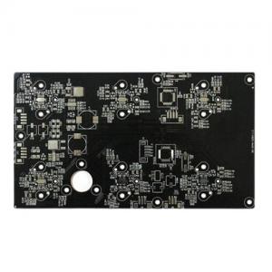
Copper Clab Black PCB Board
Copper-based PCB or copper core PCB is a metal core PCB using copper as the base material. Like all metal core PCBs, it also has three main layers. The top layer is made of copper, which is responsible for the electrical connection between the components. This layer is standard in all types of PCBs. The second layer is the dielectric layer that prevents current from the top layer to the base layer. Although this layer is electrically an insulator, it is a good conductor of heat. It transfers the heat produced by the components and helps in heat dissipation. The bottom layer of the PCB is copper, which is why it is a copper core PCB.
Copper-based PCB provide the best performance among all-metal core PCBs. These PCBs are used for particular purposes, including high-frequency circuits and high-temperature variations. They can dissipate heat better than iron and aluminum core PCBs.
| Items | Capability |
| Board Classification | Copper Base,Ceramics Base,Copper-Clad |
| Material | Copper, FR4 |
| Surface Treatment | HASL/ENIG/OSP/Silver |
| Layer Count | Single-sided printed board/Double-sided printed board |
| Max.Board Size | 1200mm*480mm |
| Min.Board Size | 5mm*5mm |
| Trace width/Space | 0.1mm/0.1mm |
| Board Thickness | 0.5mm-5.0mm |
| Copper Thickness | 35um/70um/105um/140um/175um/210um |

FAQ:
Q1:Are you a factory or trade company?
A: Yes, we are the factory, we have independent quick turn prototype PCB manufacturing & big volume PCB production lines.
Q2:What kind of PCB file format can you accept for production?
A: Gerber, PROTEL 99SE, PROTEL DXP, POWER PCB, CAM350, ODB+(.TGZ)
Q3:Are my PCB files safe when I submit them to you for manufacturing?
A: We respect customer's copyright and will never manufacture PCB for someone else with your files unless we receive written permission from your side, nor we'll share these files with any other 3rd parties. And we could sign NDA with client if necessary.
Q4:If we have no PCB file/Gerber file, only have the PCB sample,can you produce it for me?
A: Yes,we could help you to clone the PCB. Just send the sample PCB to us, we could clone the PCB design and work out it.
Q5:What is your standard lead time for PCB?
A: Sample/prototype(less than 3sqm):
1-2 Layers: 3 to 5working days (fastest 24hours for quick turn services)
4-8 Layers: 7~12 working days (fastest 48hours for quick turn services)
Mass production (less than 200sqm):
1-2 Layers:7 to 12 working days
4-8 Layers:10 to 15 working days
Q6:What payment do you accept ?
A: Wire Transfer(T/T) or Letter of Credit(L/C) or Paypal(only for small value less than 500usd)