1oz 4 Layer PCB Board Electronic PCB Assembly High Density Interconnect 1.0mm
HDI PCB Board 4 Layer PCB Board Electronic PCB Assembly High Density Interconnect Printed Circuit Boards
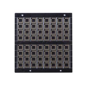
4L 1+N+1 HDI Boards
High density interconnect printed circuit boards, which are also called HDI boards, are characterized by finer lines, closer spaces, and more dense wiring.
HDI boards own higher circuit density, its designs can include not only smaller through holes and capture pads, but also higher connection pad density. They are widely used to reduce the weight and overall dimensions of products, as well as to enhance the electrical performance of the device.
HSX products cover 1~32L FR-4 PCB, IMS PCB,HDI Boards, high frequency PTFE boards and Rigid-flex boards etc. It provides flexible quick turn production services (12 hours to72 hours), as well as small volume to big volume PCB manufacturing.
Products are widely used in high-tech fields such as communications, power supplies, computer networks, digital products, industrial control, science and education, medical devices, and aerospace. HSX owns high-educated and experienced team and advanced production equipment.
The panel size of HSX factory's capability is max 740x500mm, but when the panel size is larger than 600mm, it will need to be review at first. And the minimum panel size that we can reach is 5*5mm.
The PCB thickness we can reach is from 0.2mm to 4.0mm, when the board thickness is lower than 0.2mm, or higher than 4mm, the board will need to be evaluated at first. (PS. When board thickness is equal to or less than 0.6mm, it will not apply for HASL surface finished)
The inner and outer layer's base copper thickness is smallest 0.3/0.5oz, and max 3oz.
0.15mm is factory's minumun hole size capability, when the hole size is smaller than 0.15mm, the board will need to be reviewed at first.
The colors of solder resist contain green,matt green,blue,matt blue,black,matt black,yellow,red,white, and as customer specify.
The colors of leged contain white, black and as customer specify.
| Laminate type/brand: | Shengyi FR4 | Circuit board layer: | 4 layer |
| PCB Board thick: | 1.0 MM | Different Copper thickness: | 1/H/H/1OZ |
| Smallest Mechanical drilling hole: | 0.3 mm | Finished Board profile: | Milling and V-CUT |
| Solder resist details: | YEYO Black color | Smallest line distance/space: | 4/4mil |
| Legend details: | White | surface details: | Immersion Gold |
| Special request/remark: | HDI Buried vias and blind vias, one step stack up /impedance control/resin filled and plated over |
| Circuit Board usage: | communications |

FAQ:
Q1:Are you a factory or trade company?
A: Yes, we are the factory, we have independent quick turn prototype PCB manufacturing & big volume PCB production lines.
Q2:What kind of PCB file format can you accept for production?
A: Gerber, PROTEL 99SE, PROTEL DXP, POWER PCB, CAM350, ODB+(.TGZ)
Q3:If we have no PCB file/Gerber file, only have the PCB sample,can you produce it for me?
A: Yes,we could help you to clone the PCB. Just send the sample PCB to us, we could clone the PCB design and work out it.
Q4:What is your standard lead time for PCB?
A: Sample/prototype(less than 3sqm):
1-2 Layers: 3 to 5working days (fastest 24hours for quick turn services)
4-8 Layers: 7~12 working days (fastest 48hours for quick turn services)
Mass production (less than 200sqm):
1-2 Layers:7 to 12 working days
4-8 Layers:10 to 15 working days
Q5:What is your min. order quantity?
A: There is no MOQ.The quantity will only affect the price.
Q6. How to get quick quotation?
Please provide gerber file and details of the board(including layer, board thickness, copper thickness, surface treatment, solder mask and silkscreen color, special request if any, demand quantity, etc)
sample:
| PCB Type | 4L multilayer PCB |
| Surface finished | LF-HASL |
| Base material | FR4, TG170 |
| Copper thickness | 1oz inner base, 1oz finished copper |
| PCB solder mask | Green for both sides |
| PCB silkscreen | White for both sides |
| Special requirement | Resin plugged hole/plating edge, gold finger thickness 30u" |