HASL OSP Multilayer Flex Pcb Prototype Halogen Free Immersion Tin
Rigid Flex PCB Rigid Flex PCB Design Multilayer Flex PCB Flex PCBs Multilayer Flex Circuits Flex Circuit Prototype
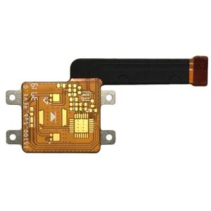
Multilayer flex rigid printed circuit board
PCB Layer: Single layer, double sided, multi-layer
PCB material: FR-4 (Standard FR4, Mid-Tg FR4,Hi-Tg FR4, Lead free assembly material) , Halogen-Free, Ceramic filled, Polyimide...
Surface finished: Immersion Tin, Immersion Silver, ENIG, ENEPIG, HASL, OSP, Hard Gold, Soft Gold(mostly ENIG)
Copper thickness: 1/3~5oz
Smasllest drilling size: 0.15mm
smallest trace/space:3mil/3mil
Solder mask: PI solder mask coverlay film or PET solder mask covelay film lamination( Black, Red, Yellow and Green, etc)
Legend: White, Black and as customer requested
Application: telecommunication product, aerospace field, military products and medical fields
Rigid PCBs' applications range from small electrical devices to large aerospace, military and medical fields. And flex printed circuit boards are built of flexible substrate. They have lower thickness, lighter weight, and they are dynamically bendable, so they can save space They also have equally vast applications because of their excellent electrical and thermal performance.
Flex-rigid PCBS are boards which combile the technology of flexible board and rigid board. They consist of multiple layers of flexible circuit substrates attached to one or more rigid boards either externally or internally. Therefore they own the advantages of both rigid printed circuit boards and flex circuit boards. Rigid-Flex products provide reliable integration of multiple rigid printed circuit board assemblies into a single PCB module capable of supporting assembly, space/weight savings, and mechanical stability.
The advantages of rigid flex board includes:
1) ruducing products' weight
2) temperature resistance is excellent
3) being more flexible
4) with good reliability
| PCB Layer | Rigid 2L + Flex 2L |
| Surface treatment | Immersion gold 3u" |
| PCB material | FR4 TG170&Polyimide |
| PCB thickness | 0.8mm+0.4mm |
| Copper thickness | 1/3oz base |
| Min. hole size | 0.20mm |
| Min. trace/space | 4mil/4mil |
| PCB solder mask | Green, both sides |
| PCB silkscreen | White, both sides |
| E-test | 100% E-Tested |
| Application | telecommunication products |
Factory's introduction:
HSX products cover 1~32L FR-4 printed circuit boards, IMS printed circuit boards,HDI printed circuit boards, high frequency PTFE boards and rigidflex boards. And we provide flexible quikturn/fast services (12 hours to 72 hours), as well as small volume to big volume PCB manufacturing.
Products are widely used in high-tech fields, lilke communication industry, power supplies industry, comsumer electronic industry, industrial control, medical devices, and so on. We own high-educated and experienced PCB team and advanced production equipments.
Max layers: 32layer (≥20 layer needs to review)
Max finish panel size: 740* 500 MM(>600 MM needs to review)
Min finish panel size: 5 * 5mm
PCB material: PI +FR4,FR4, Rogers,Halogen-free, High TG and heavy copper
PCB thickness: 0.2~4.0mm(<0.2 mm,>4 mm needs to review)
PCB copper thickness: H~5oz
Bow and twist: 0.075%
Min. hole size: 0.15mm(<0.15 mm needs to review)
Max hole size: 6.0mm(>6mm, use milling to enlarge holes)
HDI Min drill hole: 0.08-0.10MM
Min space in inner layer(one-sided): 4~8L(include): sample: 4 mil; small volume: 4.5 mil;
8~12L(include): sample: 5 mil; small volume: 5.5 mil
12~18L(include): sample: 6 mil; small volume: 6.5 mil
PCB solder mask: Green, Matt green,Blue, Matt blue, Black, Matt black, Yellow, Red, White,etc
PCB silkscreen: White, Black, etc
PCB surface: HASL lead free,Immersion Gold, Immersion Tin, OSP, ENIG + OSP, Immersion Silver, ENEPIG, Gold Finger
Application: Communications, Industry/comsumer Electronic.

FAQ:
1. What service can you provide?
PCB Manufacture,PCB Assembly,Rapid Prototype
2. How fast is your lead time?
Fastest 24H for 2L and 4L, 3WDs for HDI board.
3. How to get quick quotation?
Please provide gerber file and details of the board(including layer, board thickness, copper thickness, surface treatment, solder mask and silkscreen color, special request if any, demand quantity, etc)
sample:
| PCB Layer | 2L |
| PCB surface | LF-HASL |
| PCB material | FR4, TG170 |
| Copper thickness | 1/1oz finished |
| PCB solder mask | Double side,green |
| PCB silkscreen | Double side,White |
| Quantity | 15pcs,15 working day |
4.What payment terms do you have?
Wire Transfer(T/T)